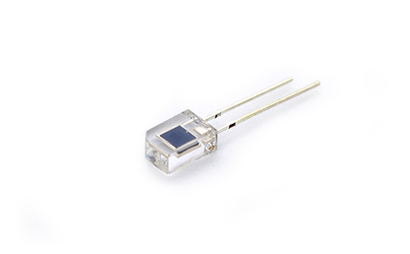
LED lamp bead packaging is mainly composed of substrate, chip, solid crystal adhesive, phosphor, packaging adhesive, etc. The substrate is then mixed with phosphor and packaging adhesive to match different phosphor ratios and appropriate chip wavelengths to obtain different colors. Finally, the mixture of phosphor and packaging adhesive is poured into the substrate, heated and baked to solidify the adhesive, completing the most basic LED lamp bead packaging. LED bead packaging mainly provides a platform for the emission of LED bead chips, enabling LED bead chips to have better optical, electrical, and thermal performance. Good packaging can make LED lamp beads have better luminous efficiency and a good heat dissipation environment, and a good heat dissipation environment can improve the service life of LED lamp beads. LED bead packaging technology is mainly based on five main considerations, namely, light extraction efficiency, thermal resistance, power consumption, reliability, and cost performance (Lm/$).
LED bead packaging technology is mainly developing towards high luminous efficiency, high reliability, high heat dissipation capacity, and thinness. From the perspective of chips, the most common ones are horizontal chips, and relatively high-end manufacturers are developing vertical chips and flip chip chips. The original horizontal array of LED beads uses a sapphire substrate, which has poor heat dissipation and requires high current drive., The light extraction efficiency also decreased significantly. Therefore, in order to reduce the cost of LED beads, high current density chip design to obtain more light output is the main research direction. With this in mind, the use of vertically packaged chips will become the topic of the next lesson. This type of chip uses high heat dissipation substrates such as silicon, which has better heat dissipation efficiency under high current operation, and therefore has higher optical output. However, due to the complex production process and low process yield, it is not possible to achieve the desired high cost performance ratio. It can be seen that in high wattage packaging, the price factor brought by process yield is also the main consideration factor. Currently, LED bead packaging technology is mainly developing in four directions: high luminous efficiency, high reliability, high heat dissipation capacity, and thinness. Currently, the main highlights are silicon based LED lamp beads and high-voltage LED lamp beads. The reason why silicon based LED beads are receiving increasing attention in the industry is that they have stronger heat dissipation capabilities than traditional sapphire based LED beads, so their power can be increased. High voltage LED lamp beads are another bright spot. It can significantly reduce the input and output voltage differential of the DC-DC step-down circuit, further improve the efficiency of the LED bead drive power supply, effectively reduce the requirements of the LED bead lamp on the heat dissipation housing, thereby reducing the overall cost of the LED bead lamp

Internal structure and working principle of infrared receiver tube

What is the principle of sensor LED beads

The structural principle and characteristics of infrared LED bead light source

Infrared LED beads based on the impact of infrared radiation on the human body
Address: 5th Floor, Building 12, Changfeng Industrial Park, Dongkeng, Fenghuang Street, Guangming District, Shenzhen, Guangdong Province
Tel: 13632942401
Email: led_best@163.com

Copyright ? 2023 Tianshi All Rights Reserved 粵ICP備2021179733號